
Tesla has outlined a new generation of custom silicon under a freshly adopted “SI” label, short for Super Intelligence, and the Tesla AI accelerator roadmap now spans inference chips from SI4 through SI6 alongside a revived Dojo training line. The plan gives the company’s hardware ambitions a clearer shape while leaving several central performance figures undisclosed.
What the SI Name Change Covers
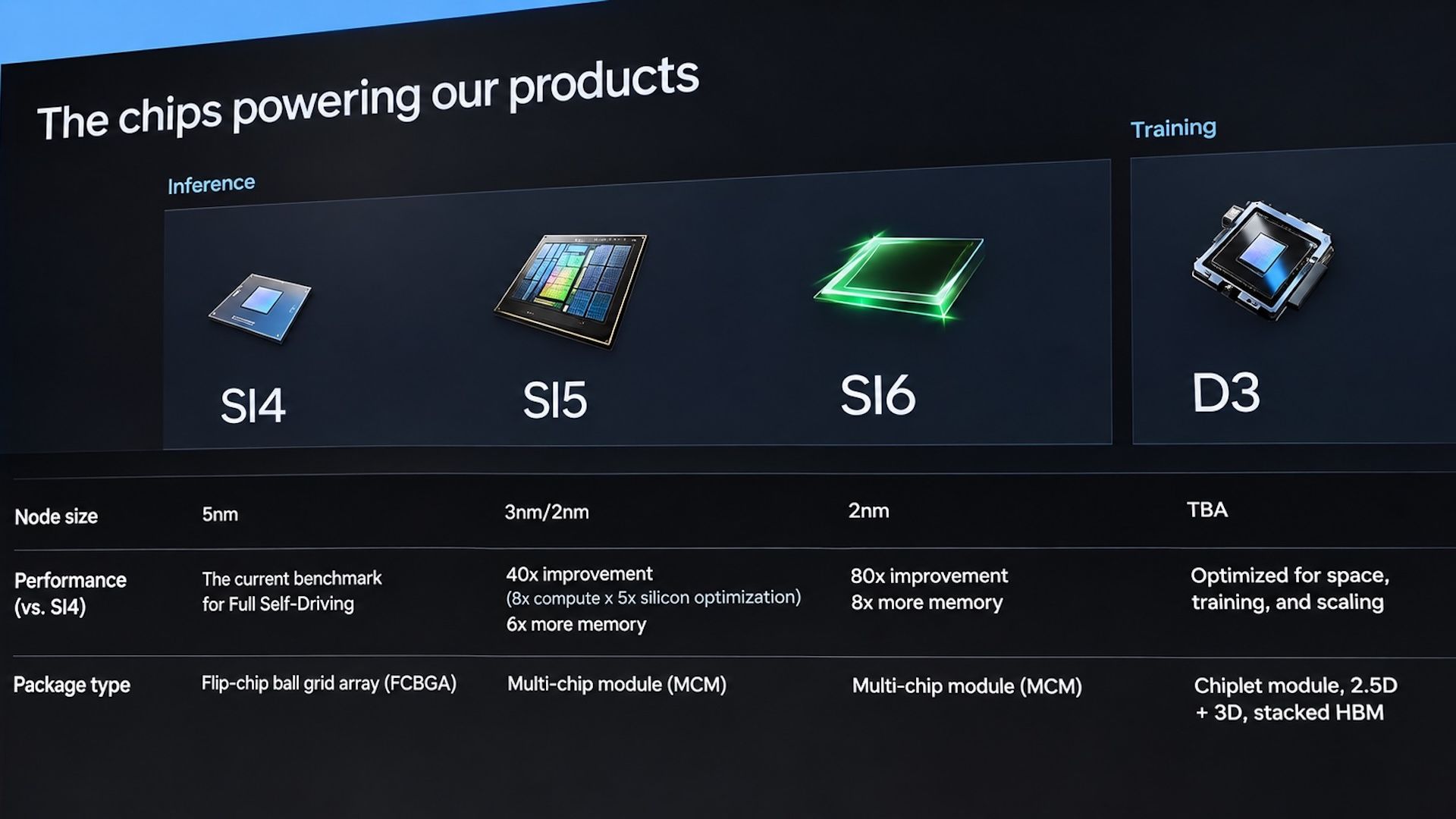
The company has replaced its earlier AI naming with SI designations across its accelerator family. The shift follows a broader preference expressed by President Trump for the term Super Intelligence over Artificial Intelligence, and Elon Musk has already applied similar branding elsewhere, with SpaceXAI set to become SpaceXSI. In Tesla’s presentation, the chips previously known as AI4, AI5 and AI6 appear as SI4, SI5 and SI6.
SI6 Targets an 80X Jump Over Today’s Hardware
Tesla expects its sixth-generation inference accelerator, SI6, to deliver 80 times the compute performance of its fourth-generation chip, which is the unit used in its vehicles today. Memory is projected to grow ninefold, pointing to roughly 144 GB. Based on estimates tied to how HW4 performance is measured, SI6 could land between 17,280 and 46,080 TOPS, or 17.28 to 46.08 POPS. Those figures are approximations, and Tesla has not detailed which data formats the chip will support.
The comparison to Nvidia’s Rubin GPU is stark in timing as well as scale. Rubin is described as shipping to customers now, while SI6 is not due until 2029–2030. Tesla has a Samsung Foundry agreement to produce its sixth-generation inference accelerators through 2033, and the roadmap places the chip on a 2nm-class process. The design is expected to retain the multi-chip module approach introduced with SI5, a choice that could let Tesla carry over packaging experience and keep costs in check.
SI4 and SI5 Set the Baseline
SI4, originally HW4 and later AI4, is manufactured by Samsung Foundry on a 7nm-class process and uses conventional flip-chip ball grid array packaging, with presumably 16 GB of GDDR6 memory. The presentation slide reportedly contains an error in labeling the process as 5nm-class. Tesla treats SI4 as the benchmark for its Full Self-Driving technology and does not officially publish its absolute compute, memory capacity or power consumption.
Musk has previously said HW4 was three to eight times more powerful than HW3, which was rated at 72 TOPS, yielding an estimated 216 to 576 TOPS for HW4. The upcoming SI5, also known as HW5 or AI5, is slated for 3nm- and 2nm-class production at TSMC and Samsung Foundry respectively and will move to a multi-chip module design. Tesla projects a 40X improvement over HW4, which Musk attributes to an eightfold compute increase from denser processes and more execution units plus a fivefold gain from silicon optimization. That points to an estimated 8,640 to 23,040 TOPS. SI5 is expected to draw 250W to 800W depending on application and to carry six times more memory than its predecessor, or 96 GB, with bandwidth between 768 GB/s and 1.536 GB/s depending on whether GDDR6 or GDDR7 is used.
Dojo D3 Returns With a Different Architecture
The most notable turn in the roadmap is the re-emergence of Tesla’s in-house Dojo training accelerator. Musk cancelled the wafer-level Dojo project in August 2025 and later said SpaceX and xAI would use Nvidia hardware exclusively in their terrestrial and extraterrestrial data centers as of August 2026. Yet Dojo D3 now appears as a chiplet-based design combining 2.5D and 3D packaging with stacked HBM.
That marks a break from Dojo D1, which relied on distributed on-chip SRAM and linked 25 D1 processors with 11 GB of SRAM each through wafer-scale packaging. HBM would address the memory capacity limits that make SRAM unattractive for modern AI models, though it brings different trade-offs in latency, bandwidth, packaging and power. Whether Tesla has abandoned wafer-scale integration entirely is unclear. Stacking custom HBM on logic dies joined by wafer-scale packaging is technically possible, but the added design complexity, cooling demands, manufacturing risk and cost make it less likely for D3.
Tesla has not disclosed D3’s compute performance, memory capacity, manufacturing process or development schedule. The company says the chip will be optimized for space, training and scaling, language that suggests a more conventional, easily scaled accelerator design. The space optimization also implies radiation hardening for at least some SKUs.
Open Questions Remain
Tesla’s roadmap sketches a multi-year path from today’s inference silicon to far larger chips, but it leaves key details unsettled. The SI6 timeline places it years behind current Nvidia hardware, the D3 architecture raises questions about wafer-scale packaging, and Tesla has not said when HBM might reach its inference accelerators, though probably not with SI6. For now, the SI branding and the revived Dojo line define the direction more than the final specifications do.