
Nagare Labs, a Georgia Tech spinout with Pat Gelsinger on its board, is promoting Z2RAM memory-on-compute as a way to place memory with SRAM-like speed and DRAM-like density directly atop AI accelerators. The concept rests on capacitorless gain cells built from two transistors and a shield, deposited in stacked layers on the compute die. But the published work behind it remains at the laboratory stage, and the company has yet to demonstrate a fabricated multi-layer stack.
What the founders' papers show
The technical case comes largely from peer-reviewed work by co-founders Suman Datta and Shimeng Yu and their groups. A 2020 tungsten-doped indium oxide two-transistor cell retained data for 1 second at 25°C but only 300 milliseconds at 85°C. A 2025 update added a third transistor and removed gate overlap, reaching more than 1,000 seconds at room temperature. A later “folded asymmetric boosted” three-transistor cell held data for over 300 seconds at 85°C, compared with about 100 milliseconds for a conventional three-transistor design. That boosted cell is described as refresh-free, meaning cached data would not decay before being overwritten.
Those retention figures still fall short of the roughly 95°C threshold Nagare says DRAM must stay below. Neither the published cells nor Z2RAM itself have shown retention above that line.
Projected gains versus measured results
Nagare’s Gen 1 projections call for five times the density of SRAM across six stacked layers, 14 times the speed of DRAM, and one-third the read energy of SRAM. The company also targets well under a picojoule per bit. These are projections, not measurements of a completed product.
Simulations from the founders’ groups offer some supporting context. A four-tier, 256MB cache of two-transistor gain cells at 7nm was simulated to reach 5.7 times the bit density of 7nm SRAM in the same area. A simulated GPU L2 with twice SRAM’s capacity in the same area showed a 75–80% lower energy-delay-area product. The boosted cell is projected at 0.0168 µm² at 7nm, smaller than a high-density SRAM cell on TSMC’s 3nm process at 0.0199 µm². A simulated read delay of 2.6 ns and a measured 10 ns write pulse round out the published figures.
The thermal ceiling on stacked memory
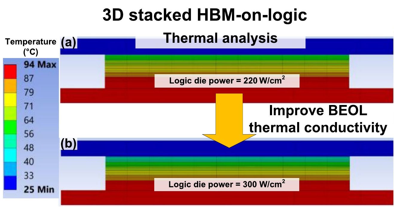
Heat is the central constraint for any memory stacked on logic. A 2025 simulation by Yu’s group found that with HBM stacked on a logic die, keeping DRAM at or below 95°C caps logic power at 220 W/cm², or 300 W/cm² with improved thermal vias. That limit is already influencing commercial designs: Micron’s vHBM plans include heat-spreading structures, and Samsung’s zHBM is planned at only about four layers. Nagare’s approach would face the same thermal physics.
Manufacturing without a fab
Nagare says it can pattern memory layers together on one die using standard 300mm DUV tools, with no EUV and no interposer or bonds between layers. A single lithography exposure would cover several layers, potentially avoiding the mask-cost penalty that makes additional tiers uneconomical past seven or eight layers. The roadmap aims at more than 100 layers and hundreds of thousands of vertical connections.
None of that has been proven in a manufactured stack. Datta has described the work as laboratory prototypes. Sampling of Z2RAM tiles is targeted within four years, with production shipments, if they arrive, within the next decade. Nagare currently has no fab and is reportedly seeking an R&D fabrication partner to scale beyond university clean rooms. Yu has noted that no standard exists for integrating this kind of memory with an accelerator, which could force Nagare to define its own interface. Reliability also remains open, as single-electron effects can shift a cell’s threshold enough to corrupt stored bits. It is also unproven whether the tested three-transistor cells will perform adequately as a two-transistor, single-shield product.
Lineage and competition
Z2RAM is not the first capacitorless memory to claim a fivefold density advantage over SRAM. Innovative Silicon’s Z-RAM, licensed by AMD two decades ago, made a similar pitch but was not pursued. A separate Georgia Tech paper due at IEDM in December covers a one-transistor, one-ferroelectric-transistor cell aimed at the same latency-density gap. High-bandwidth flash, which stacks NAND like HBM beside the GPU, is another alternative still in development.
Gelsinger’s involvement connects the effort to a broader memory debate. As Intel’s chief executive, he phased out Optane, a low-latency non-volatile memory, in favor of CXL. Now a general partner at Playground Global, which led Nagare’s $5 million round, he sits on the startup’s board as it pursues a different answer to the memory wall. Nagare declined to share measured retention, latency, or energy figures. Until a fab-built, multi-layer Z2RAM stack is measured, including retention above 95°C, its headline numbers remain projections.