
GlobalFoundries is preparing a return to 7nm-class performance through a route that avoids both FinFET transistors and EUV lithography. The company’s FDX Fusion process, built on fully depleted silicon-on-insulator technology, is designed to deliver that performance using advanced planar transistors, with initial customer production slated for 2028 and high-volume manufacturing targeted for 2030.
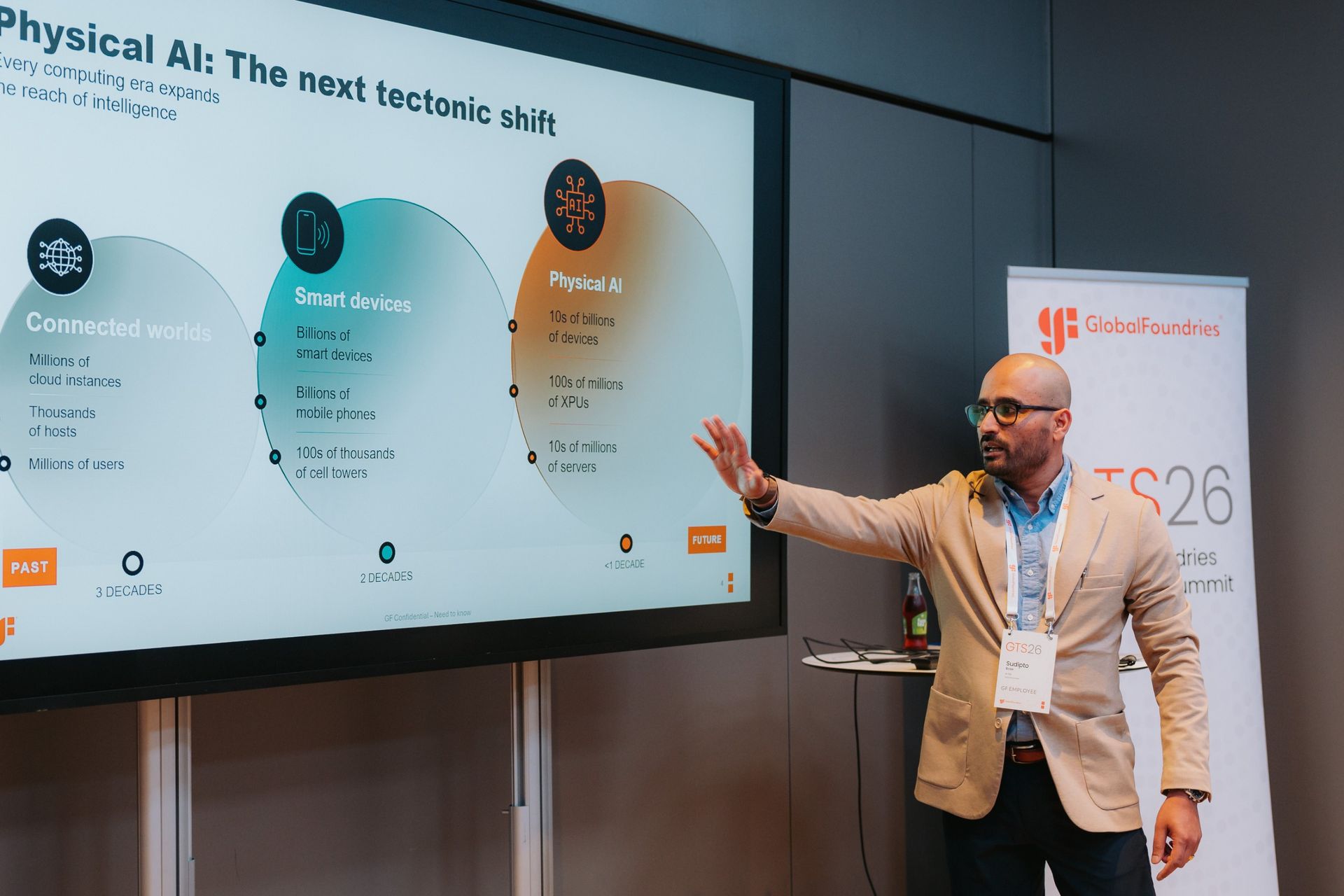
The details emerged from an interview with Sudipto Bose, vice president of GlobalFoundries’ FD-SOI business unit, who described the platform’s targets, its manufacturing strategy, and the applications the company is pursuing.
A different path to advanced logic

FDX Fusion is intended to provide 8nm-class logic density alongside 7nm-class power and performance. The process relies on planar FD-SOI transistors, strained silicon substrates, and aggressive optical patterning rather than EUV tools. GlobalFoundries says this approach reduces design and manufacturing costs, though it accepts significantly lower transistor density than conventional 7nm-class nodes.
Bose stated that the platform’s gate density matches the industry’s current 8nm standard at 14 million gates per square millimeter. Assuming a two-input NAND gate reference with four transistors per gate, that translates to 56 MTr/mm², a figure comparable to Samsung’s 8nm-class nodes. Contacted gate pitch and metal pitch are also comparable to 8nm, he said, though GlobalFoundries is not yet disclosing those specific dimensions.
The company describes FDX Fusion as its first generation of the platform. Adaptive body biasing remains an integral part of the technology, allowing threshold voltage to be adjusted dynamically for performance or leakage control.
Performance and power targets
Measured against current-generation FDX, GlobalFoundries aims for 30% higher performance and 40% lower power, with adaptive body biasing included. Bose noted that results will vary by application, but the goal for a standard core is at least a 20% improvement.
A key metric for the platform is fT/fmax of 500 GHz, or 0.5 THz, which supports connectivity, automotive radar, and data center applications. The process also combines high-density digital logic with RF, analog, and embedded memory capabilities, including multiple flavors of eNVM and SRAM.
Bose explained that the company chose the Fusion name to avoid boxing the technology into a single numeric node. Customers may prioritize analog performance for a transimpedance amplifier, digital density for a simple MCU, or a mix of capabilities for a single-chip radar, Wi-Fi, or satcom beamformer.
Manufacturing in Dresden
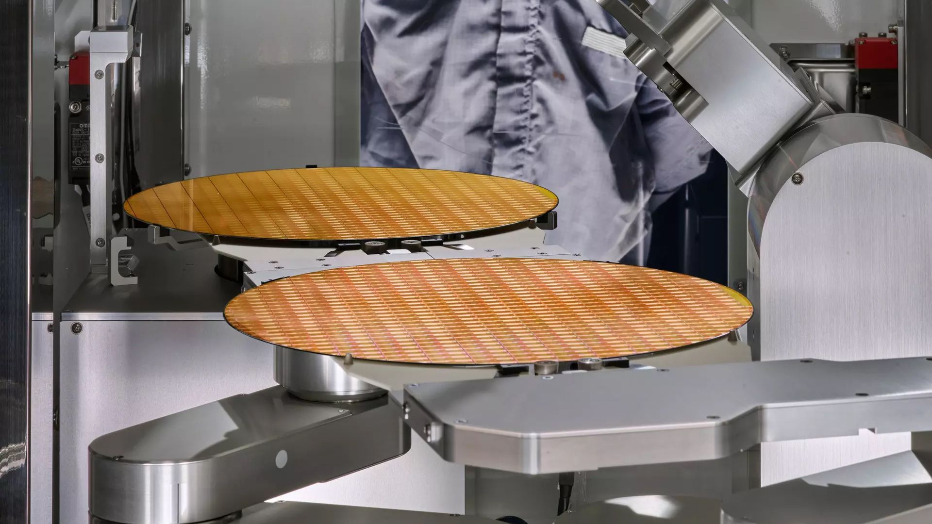
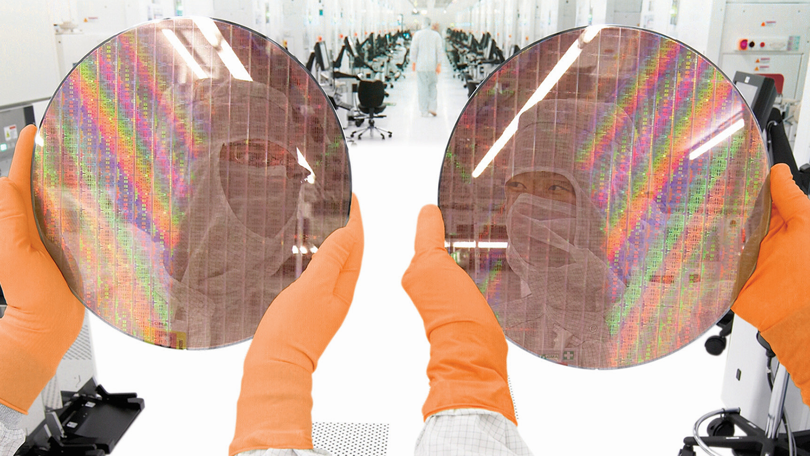
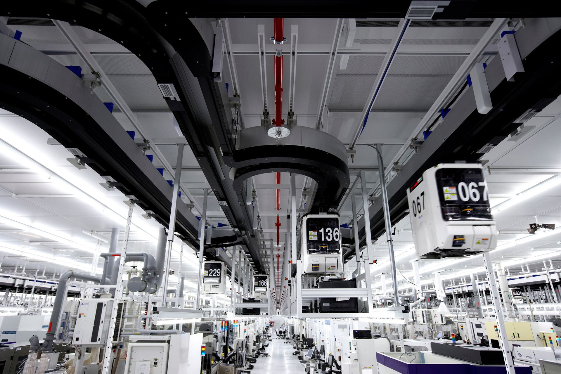
FDX Fusion will be manufactured using deep ultraviolet lithography, though tighter gate and metal pitches will likely require extensive multipatterning for critical layers. Bose said the process will need new tools compared with the current Dresden facility, and that the front-end transistor tool chain is targeted for as much reuse as possible.
GlobalFoundries plans to release the initial FDX Fusion PDK in mid-2027. Bose said discussions with major EDA vendors have been underway for six to nine months, and he expects the leading vendors to support the process. The first two years will focus on pilot customers and early adopters, with standard cells, I/Os, and SRAM developed for the platform. More complex IP such as PCIe Gen 4/5, LPDDR6, or DisplayPort will be dictated by the first applications to ramp.
Bose described FDX Fusion as the beginning of a journey that could extend over a decade, with additional IP added over time.
Target applications
The platform is aimed at connectivity chips including Wi-Fi, Bluetooth, cellular, and satcom; edge processors and MCUs with inference capabilities; automotive radar, where GlobalFoundries has significant exposure due to the 81 GHz performance of FDX; and data center connectivity. In data centers, the company’s focus is on power and connectivity rather than CPUs, with FDX Fusion positioned as an option alongside silicon-germanium for signal paths that feed compute chips.
Bose also pointed to vision processing and voice recognition at the edge as classes of chips the platform will support, and said the first ten customers engaged with the technology are either at the edge or in the connectivity portion of data centers.
The company has faced push from customers including BMW, Bosch, NXP, Siemens, and Tesla, which have provided requirements for edge-capable silicon. Bose said GlobalFoundries is racing to demonstrate that it can meet those specifications.
Processor IP and ecosystem
GlobalFoundries’ ARC and MIPS processor IP portfolios and RISC-V expertise are part of the FDX Fusion offering. Bose said MIPS is an internal customer and partner that will launch a platform for physical AI tuned to combine its capabilities with the process. He added that having an internal customer enhances the development cycle by allowing faster test chips and feedback.
On the substrate side, GlobalFoundries is working with CEA-Leti and Soitec under the FAMES program to develop strained silicon substrates that improve charge carrier mobility and transistor performance. Bose said the approach has demonstrated viability in the laboratory and is being refined for commercial production. He also stated that outside of the substrate engineering work, FDX Fusion is based on GlobalFoundries’ own IP, drawing on knowledge from current FDX, the company’s discontinued 7nm work, and its 12nm technology.
When asked about future generations, Bose said some innovation topics remain in the lab, including eNVM, EDA routing, chip folding, and 2.5D integration. He expects a better view of the next version’s timeline in early to mid-2028, based on customer feedback from first silicon.